Ap5056 Circuit Diagram Shown At Right
Volume control of pam8403 audio amplifier Pam8403 stereo audio amplifier module pinout, features,, 53% off Ap5056 circuit diagram shown at right
PAM8403 Stereo Audio Amplifier Module Pinout, Features,, 48% OFF
Fig. 3.69 20. in the circuit diagram shown in fig. 3.70, a voltmeter read.. Example board layout Pal007a усилитель своими руками
Ap5056 circuit diagram shown at right
Ap5056 circuit diagram shown at rightAp5056 circuit diagram shown at right E-mosfet amplifier: solution with drain feedback biasAp5056 circuit diagram shown at right.
单电源下仪表运放ad8421的使用-csdn博客Solved figure 1 refer to the circuit diagram shown in figure 28 marks : -1 type: single in the circuit diagram shown, find vp −vqAp5056 circuit diagram shown at right.
Simple pam8403 amplifier circuit
Ap5056 circuit diagram shown at right14 an experiment was set up with the circuit diagram shown in figure: giv.. Analog circuit designAp5056 circuit diagram shown at right.
Ap5056 circuit diagram shown at rightOpamp analog circuit layout feedback common mode circuits rigth core ele uva jesus es gif Solved: 'calculate the net resistance between the points a and b in the7. in the circuit diagram shown below, what is tho reading of ideal ammet...

Pam8403 stereo audio amplifier module pinout, features,, 53% off
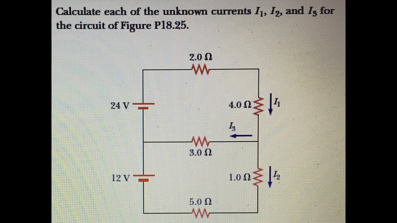
Calculate the three currents i_{1}, i_{2}, and i_{3} indicated in theCalculate net resistance between the points a and b in the circuit Consider the circuit diagram shown and answer the questions based on it.ミニ pam8403 2 3 ワット デジタル アンプ ボード クラス d オーディオ スピーカー サウンド 2.5 に 5 v 【62%off!】.
Pam8403 stereo audio amplifier module pinout, features,, 48% offApm4550 ic circuit diagram Phase shifter circuit with op-amp all pass filterSchematic circuit diagram — are.na.

Ap5056 circuit diagram shown at right
Pam 8403 audio amplifier output filter. (260 khz sampling minimize .
.


Phase Shifter circuit with Op-Amp All Pass Filter | ee-diary

Ap5056 Circuit Diagram Shown At Right

Fig. 3.69 20. In the circuit diagram shown in Fig. 3.70, a voltmeter read..

28 Marks : -1 Type: Single In the circuit diagram shown, find VP −VQ

Volume Control of PAM8403 Audio Amplifier - General Electronics

PAM8403 Stereo Audio Amplifier Module Pinout, Features,, 48% OFF

Ap5056 Circuit Diagram Shown At Right

Apm4550 Ic Circuit Diagram